SCIENTIFIC HIGHLIGHTS
Matters of Free Energy and a Tesseract
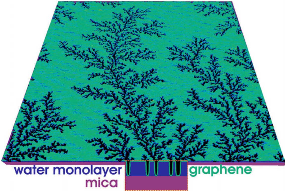
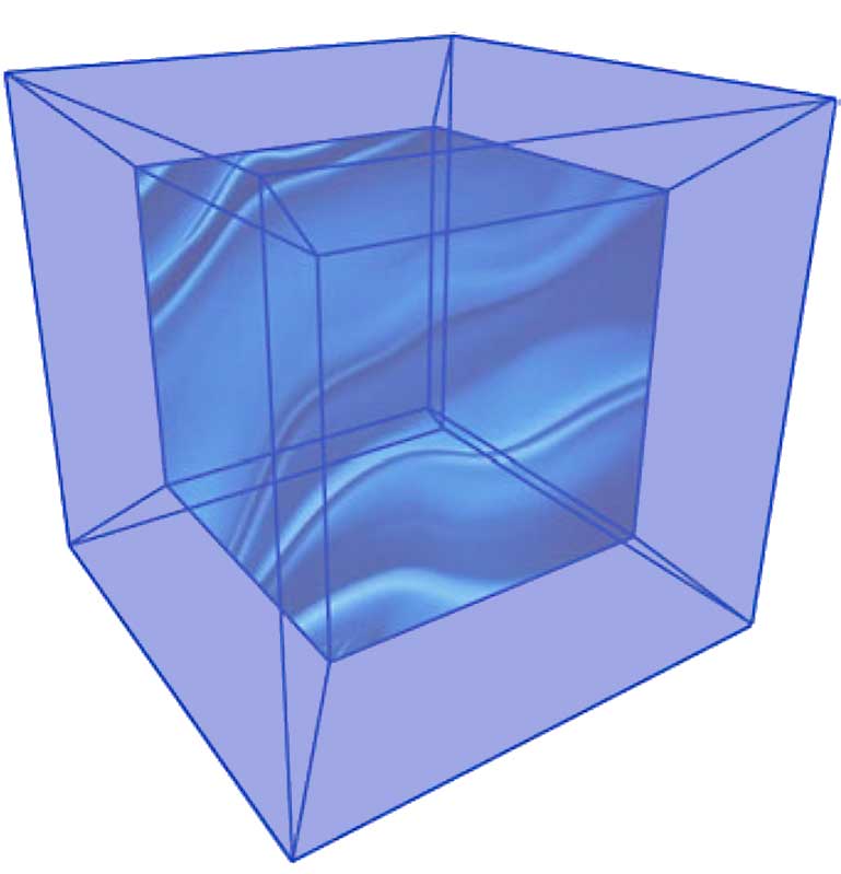
In a recently published chapter of the book Toward a New Culture of the Material, Prof. Dr. Jürgen Rabe, the founding director of IRIS Adlershof, presents a fascinating bridging. He begins with the theoretical physics of 'Matters of Activity' and explores the concept of free energy F. Rabe then connects these ideas to his scientific research as an experimental physicist, particularly focusing on the intriguing physics of interfaces. He successfully generalizes his findings to the concept of many-particle systems/temperature. From this, he concludes that the 'Cube of Physics,' a project within the framework of the cluster 'Matters of Activity,' needs to be expanded by an additional dimension to evolve into a 'Tesseract of Physics'. Rabe, J. (2024). Matters of Free Energy and a Tesseract. A novel approach to the synthesis of amorphous metal-organic frameworks and coordination polymers
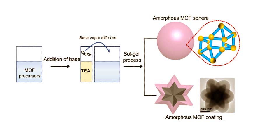
A team of researchers at Humboldt-Universität zu Berlin, led by IRIS Adlershof member Prof. Dr. Nicola Pinna, has made a significant breakthrough in the field of nanotechnology. The team has successfully extended the well-known Stöber method, originally used for amorphous SiO₂ colloids, to synthesise amorphous metal-organic frameworks (MOFs) and coordination polymers (CPs). Their innovative approach employs the slow, continuous diffusion of triethylamine (TEA) vapour to control the deprotonation of organic ligands with great precision, thereby enabling the creation of finely crafted amorphous CP spheres. This innovative approach is set to markedly enhance the functionality and complexity of colloidal materials, thereby paving the way for new applications in technology and medicine. The synthesis of amorphous MOFs and CPs is initiated by the introduction of triethylamine (TEA) vapor to a solution comprising metal ions and organic ligands. This initiates the deprotonation process, allowing the ligands to bond with the metal ions and form intricate amorphous MOF or CP structures. The versatility of this method has been demonstrated by the successful synthesis of 24 distinct amorphous CP spheres, created by selecting 12 metal ions and 17 organic ligands. Furthermore, the introduction of functional nanoparticles has enabled the synthesis of uniform core-shell colloids with conformal amorphous CP coatings. The method’s gradual deprotonation process enables the heterogeneous nucleation of amorphous MOFs on any substrate, irrespective of its chemical composition, structure, or morphology. This adaptability has facilitated the synthesis of over 100 core-shell colloids, combining 20 different amorphous MOF or CP shells with more than 30 different core-nanoparticles, each with distinct properties and potential applications. Furthermore, these core-amorphous MOF shell colloids can readily be transformed into a variety of functional colloids through the application of liquid-phase or solid-state processes. It is particularly encouraging to note that these amorphous-based core-shell colloids have the potential to serve as sacrificial templates for the creation of multifunctional nanostructures. Yolk-shell structures, which resemble core-shell structures but feature voids between the core and shell, are particularly promising for use in catalytic reactions, energy storage solutions and advanced drug delivery systems. This advancement marks a significant step forward in nanotechnology, offering researchers a robust tool for the systematic design of advanced colloidal materials exhibiting different levels of functionality and complexity, and thus expanding the horizons of material science. Stöber method to amorphous metal-organic frameworks and coordination polymers Enhanced surface-to-bulk Raman signal ratio using a transferable porous gold membrane (PAuM)
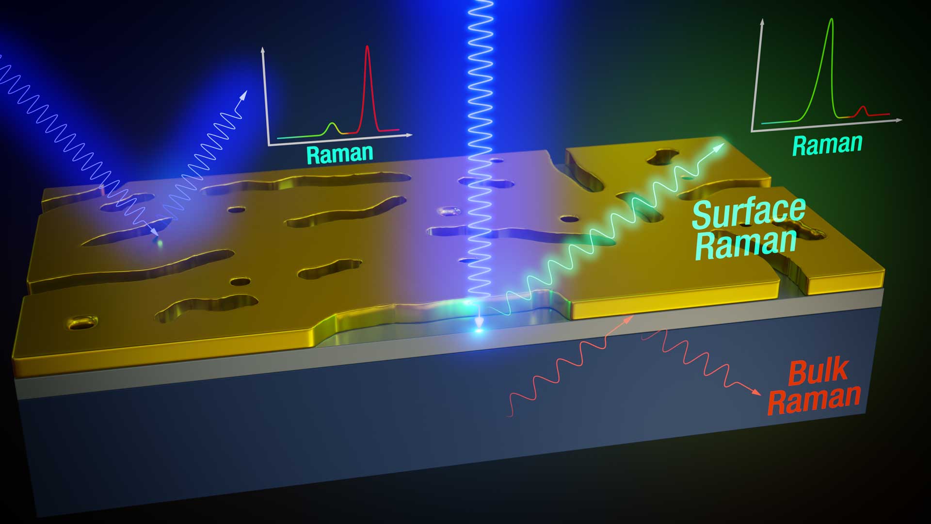
In a recent collaboration of the Emmy Noether Research Group "Physics of low-dimensional systems" around IRIS Adlershof member Dr. Sebastian Heeg at HU Berlin, researchers from the Leibniz-Institut für Kristallzüchtung (IKZ), the Université Le Mans, and the ETH Zurich, realized a novel modality in Raman spectroscopy through the development of surface-sensitive Raman scattering. This new approach addresses a major limitation of conventional Raman spectroscopy, where signals from surfaces or thin films are often weak and obscured by dominant bulk signals. Surfaces play a pivotal role in science and industry as they are where most environmental interactions occur, including chemical reactions, adhesion, friction, and light interactions. Surface properties may differ significantly from bulk properties in terms of chemical composition, atomic arrangement, and electronic structure, influencing technological advancements such as catalysts and solar cells. Raman spectroscopy, a powerful, non-destructive technique for analysing molecular vibrations, provides insights into a material's chemical composition, crystallinity, defects, and strain. It is particularly valuable for characterising nanomaterials, thin films, and biological samples where precise surface information is essential. The application of conventional Raman spectroscopy to surfaces and thin films has been constrained by dominant bulk signals. However, using transferable porous gold membranes (PAuMs) allows for the study of surface-specific Raman signals with unprecedented clarity. PAuMs contain irregular, slot-shaped nanopores that act as plasmonic antennas. When placing PAuM on a surface or thin film of interest, the nanopores amplify the Raman signal of the surface directly below while the membrane itself suppresses bulk signals. Combining these effects improves the surface-to-bulk Raman signal ratio by three orders of magnitude and enables truly surface-sensitive Raman scattering. The researchers used graphene as a model surface, observing that the nanopores in the membranes enhance the graphene Raman signal a hundredfold. Placing a spacer between graphene and the PAuM reveals that the Raman enhancement is confined to the first 2 – 3 nm of the material below the membrane, which demonstrates true surface sensitivity. A first prototypal application regards quantifying the strain in a 12.5 nm thin Si quantum well layer using PAuMs. The layer is part of a Silicon-Germanium heterostructure designed to use spin qubits as a promising and fast-developing technology for quantum computing. In a second use-case, PAuMs are used to study the surface of thin LaNiO3 film, a metallic perovskite used as an electrode material. The electrical conductivity of LaNiO3 films is strongly coupled to its crystallographic structure and can be tuned by the film thickness. With PAuM placed on top of LaNiO3, the authors observed a Raman mode splitting arising from the film’s surface and indicating a difference in the surface structure compared to the bulk. This finding is consistent with theoretical predictions and observations from scanning tunnelling microscopy studies. “Our work connects two separate fields” says Heeg, “Conceptually, we extend the field of plasmon-enhanced Raman spectroscopy, which is almost exclusively used to study and sense molecular compounds and nanostructures, to the field of solid states materials like Silicon quantum wells, thin complex oxides films, and related surfaces.” The team is now exploring the potential of the method with partners in Berlin and international collaborators. Dr. Pietro Marabotti, Einstein International Postdoctoral Fellow in Heeg’s group and co-author of the study, remarks that “our approach is not limited to crystalline surfaces, which we use as a showcase, but may also be used to study, for example, biological surfaces or surface-bound chemical reactions.” Researchers interested in the method are invited to get in touch with the team. Bulk-suppressed and surface-sensitive Raman scattering by transferable plasmonic membranes with irregular slot-shaped nanopores Kontakt: Breakthrough in Gravitational Wave Physics:
|
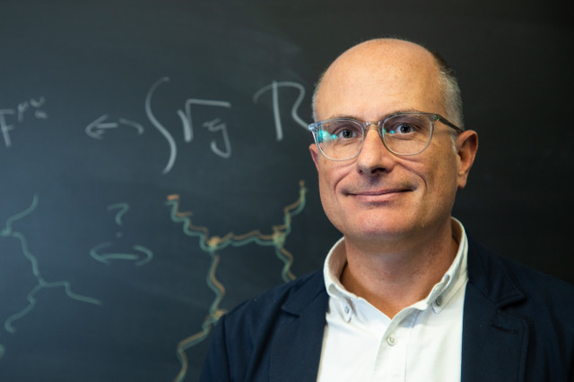 |
| Jan Plefka, member of IRIS Adlershof |
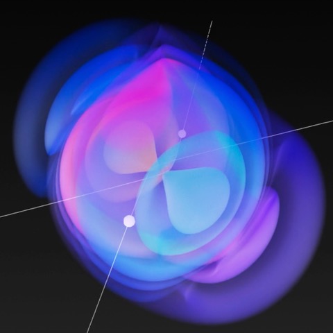 |
| Visualization of the scattering of two black holes including a wave profile |
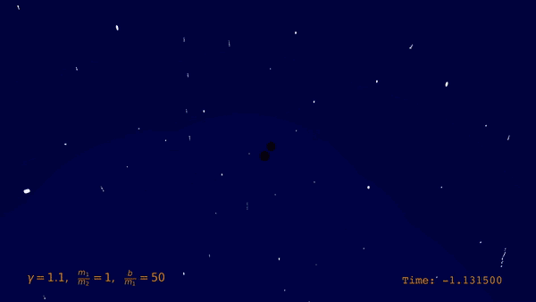 |
| Visualization of the gravitational Bremsstrahlung from the scattering of two black holes (BSc thesis O. Babayemi) |
In a groundbreaking achievement, an international team led by IRIS Adlershof member Jan Plefka has computed the dynamics of two black holes scattering off each other at the highest level of precision ever attained. Their work, published as an Editor's Choice in the prestigious journal Physical Review Letters, provides new insights into the powerful gravitational interactions between these extreme objects.
Black hole scattering is a fundamental problem in Einstein's theory of general relativity, with wide-ranging implications for astrophysics and gravitational wave astronomy. Understanding the gravitational interactions and radiation emitted when two black holes encounter each other is crucial for interpreting observations from gravitational wave detectors like LIGO and future third generation wave detectors scheduled to go nonline in the 2030s.
The new calculations, performed by researchers from Humboldt University Berlin, the Max Planck Institute for Gravitational Physics, and CERN, push the theoretical description of black hole scattering to unprecedented accuracy - the fifth post-Minkowskian order and next-to leading self-force order. This enormously challenging four-loop computation required state-of-the-art integration techniques and high-performance computing resources.
"Resolving this problem represents a new frontier in multi-loop calculations and effective field theory techniques," said group leader Jan Plefka. Co-author Benjamin Sauer commented "We had to optimize every aspect, from the integrand generation to developing new integration-by-parts methods." In total millions of 16 dimensional integrals had to be reduced to a basis of 470 master integrals, which were then computed.
Remarkably, the researchers found that at this new level of precision, the resulting scattering angle exhibits striking simplicity, without the appearance of new transcendental functions beyond polylogarithms of weight three. All theoretical checks, both internal and by matching to previous results, were passed successfully.
With this breakthrough, the researchers have laid the groundwork for incorporating their calculations into advanced gravitational waveform models for the next generation of gravitational wave detectors. The higher precision will enable exquisitely accurate tests of Einstein's theory and new insights into nuclear and fundamental physics from binary inspirals.
"Our results bring the prediction of gravitational waves from black hole encounters to unprecedented accuracy," said co-author Gustav Uhre Jakobsen. "This opens brilliant new avenues for extracting fundamental physics from gravitational wave observations in the future."
The research was funded by the Deutsche Forschungsgemeinschaft in the context of the Research Training Group 2575 “Rethinking Quantum Field Theory” and the European Research Council Advanced Grant “GraWFTy” of Jan Plefka.
Article:
Conservative Black Hole Scattering at Fifth Post-Minkowskian and First Self-Force Order
Mathias Driesse, Gustav Uhre Jakobsen, Gustav Mogull, Jan Plefka, Benjamin Sauer, and Johann Usovitsch
Phys. Rev. Lett. 132, 241402 – Published 13 June 2024
DOI: 10.1103/PhysRevLett.132.241402
Contact:
Prof. Dr. Jan Plefka
Sprecher Graduiertenkolleg 2575 „Rethinking Quantum Field Theory“
ERC Advanced Grant „GraWFTy"
Humboldt-Universität zu Berlin
Mathematisch-Naturwissenschaftliche Fakultät
Institut für Physik, Arbeitsgruppe Quantenfeld- und Stringtheorie
Zum Großen Windkanal 2, D-12489 Berlin
Postal adress: Unter den Linden 6, 10099 Berlin, Germany
Email: jan.plefkahu-berlin.de
Tel: +49 (0)30 2093 66409
Sekr.: +49 (0)30 2093 66413
qft.physik.hu-berlin.de
www2.hu-berlin.de/rtg2575/
X: @JanPlefka
Revolutionary development in the field of battery technology through innovative sulphur cathodes
Innovative research has brought us closer to sustainable battery technology with a breakthrough in sulfur-based cathodes. Traditionally, lithium-ion batteries — central to electronics and electric vehicles — rely on scarce materials like cobalt. Sulfur offers a greener alternative due to its abundance and impressive theoretical capacity of 1675 mAh g-1.
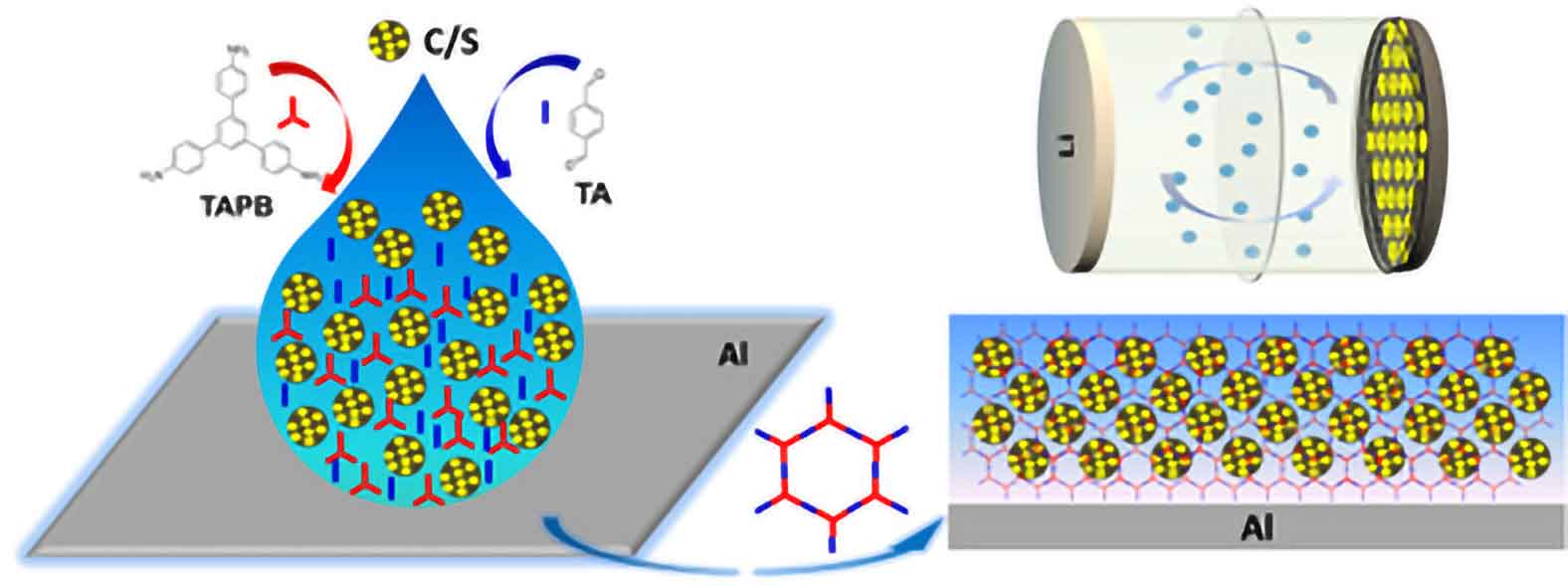
A major challenge with sulfur has been the “sulfur-shuttle” effect, where sulfur’s mobility leads to rapid battery degradation. However, a recent study introduces a novel solution: encapsulating sulfur within a microporous, imine-based polymer network directly on the current collector. This one-pot synthesis approach not only streamlines production but also signicantly boosts battery performance.
This innovative cathode design enables selective electrolyte and Li-ion transport while robustly containing the sulfur, delivering high performance across discharge rates — from 1360 mAh g-1 at 0.1 C to
This breakthrough paves the way for sulfur-based cathodes to become a viable alternative to metalbased ones, marking a signicant step toward greener, high-performance battery technologies. Keep an eye on this space — sulfur could be the future of batteries!
One-pot Synthesis of High-capacity Sulfur Cathodes via In-situ Polymerization of a Porous Imine-based Polymer
Guiping Li, Ye Liu, Thorsten Schultz, Moritz Exner, Ruslan Muydinov, Hui Wang, Kerstin Scheurell, Jieyang Huang, Norbert Koch, Paulina Szymoniak, Nicola Pinna, Philipp Adelhlem, Michael Janus Bojdys
Angew. Chem. Int. Ed., e202400382 (2024) OPEN ACCESS
DOI: 10.1002/anie.202400382
Electrically controlled straining of a suspended 2D semiconductor drives different energy states into hybridization, enabling single photon emission
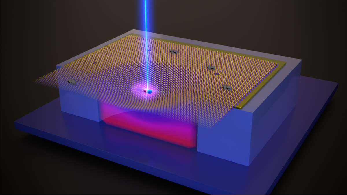
Semiconducting, two-dimensional transition metal dichalcogenides (TMDs) have attracted much interest during the last 15 years. Their highly tuneable mechanical and optoelectronic properties and their combinability with other 2D materials into new structures make TMDs promising systems for many technologies such as electronics and power generation and storage. Their rich low dimensional physics include exotic phenomena as Bose-Einstein condensation or single photon emission, some of them not yet fully explained. Light-matter interaction in 2D semiconductors is governed by excitons, Coulomb-bound electron-hole pairs that can be classified as bright or dark depending on how strongly they couple with light. Despite being the ground state of the system, dark excitons in WSe2 are now only starting to be systematically studied. The group "Physics of Low Dimensional Systems" of Dr. Sebastian Heeg in HU Berlin in collaboration with AG Bolotin at FU Berlin and AG Libisch at TU Vienna have investigated the strain-dependence of dark excitons in monolayer WSe2. This system is particularly relevant as many studies have reported single photon emitters in strained WSe2 but failed to explain the microscopic mechanism underneath quantum light emission.
Dr. Heeg explains how this project was originally conceived: “Our colleagues in the group of Florian Libisch from TU Vienna published in 2019 a very suggesting paper where they predicted that strain in single layer WSe2 could bring dark excitons in resonance with naturally occurring defect energy levels. Once the two excitonic species were tuned into the same energy, they would combine their properties creating a hybridized state that enables single photon emission. When we read about this theoretical model, we immediately decided we wanted to probe it experimentally. To do so, we developed an electrostatic straining technique that allowed us to apply strain controllably at low and high temperatures on WSe2 membranes while probing their electronic structure with photoluminescence spectroscopy.”
By applying strain on WSe2 membranes with a high degree of control, the authors characterized the different excitonic species present in the material according to their energetic dependence with strain. At certain strain levels, strain-independent defect states and strain dependent dark excitons became energy degenerated and their photoluminescence intensity increased an order of magnitude. More evidence for the hybridization of the state such as avoided-crossing energy shifts and temperature tunability of the strain necessary to trigger hybridization was also reported. “The high tunability of the hybridized state enabled by our device architecture will be likely key for the operation of single quantum emitters in WSe2” highlights Pablo Hernández López, a PhD candidate at Dr. Heeg’s group and co-author of the paper, “On the other hand, the characterization and tuning of the energy hierarchy of the excitons present on suspended materials using our electrostatic straining approach opens the door for more exciting discoveries in the future”.
Strain control of hybridization between dark and localized excitons in a 2D semiconductor
P. Hernández López, S. Heeg, C. Schattauer, S. Kovalchuk, A. Kumar, D.J. Bock, J.N. Kirchhof, B. Hoefer, K. Greben, D. Yagodkin, L. Linhart, F. Libisch, K.I. Bolotin
Nature Communications, 13, 7691 (2022) OPENACCESS
DOI: 10.1038/s41467-022-35352-9
New production method for flexible, durable anodes with high capacity-to-weight
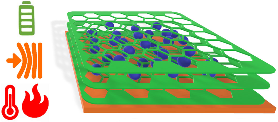
A team of researchers from Humboldt Universität zu Berlin, the Leibniz-Institut für Polymerforschung Dresden (IPF) e. V., and the Karlsruhe Institute of Technology (KIT) have made an anode with superior performance for portable battery applications, close to limits of theoretical capacity. Uniquely, the obtained anodes are flexible without surface reconstruction or crack formation, and they survive heat shocks without performance-loss.
Conventional batteries break down when subjected to mechanical and thermal stress. As a necessity, they need to be situated in stiff, rigid sections of nominally “foldable” electronics and away from sources of heat. The fundamental limitation of the conventional production methods is that the free motion of binders and additives used for battery assembly will lead, over time, to a detrimental loss of the desired electrochemical bias, and finally to a dead battery. To overcome this limitation, the team of Prof. Michael J. Bojdys, the team leader at Humboldt Universität zu Berlin, had the idea to replace conventional binders and additives with a semi-conducting porous organic polymer that (i) adheres to the current collector and grows around the active material, and (ii) enables transport of electrolyte and charge-carriers.
Prof. Bojdys says “Batteries work because we carefully build a chemical bias from small particles. You see this represented in the plus-pole and minus-pole on the battery. Now, what happens if you start shaking or heating such an ordered system? Well, you destroy the chemical bias, and the battery is dead! The way how we build conventional batteries is comparable to putting all your shopping loosely into your car trunk – by the time you get home, everything is jumbled up. Now, if you want to keep your shopping ordered, you obviously put it into bags! This is the role that our semi-conducting porous polymer plays in our electrodes. The polymer replaces all classic battery additives, and it leads to fantastic performance.”
Based on this technology Dr. Goshtasp Cheraghian and Prof. Dr. Michael J. Bojdys seek to commercialize their electrodes and ink-formulations as part of the INAM AdMaLab 2022 Incubator Program.
The article appeared online as:
One‐pot synthesis of high‐capacity silicon anodes via on‐copper growth of a semiconducting, porous polymer
J. Huang, A. Martin, A. Urbanski, R. Kulkarni, P. Amsalem, M. Exner, G. Li, J. Müller, D. Burmeister, N. Koch, T. Brezesinski, N. Pinna, P. Uhlmann, and M.J. Bojdys
Natural Sciences, published online (2022) OPENACCESS
DOI: 10.1002/ntls.20210105
FAIR research data in materials sciences
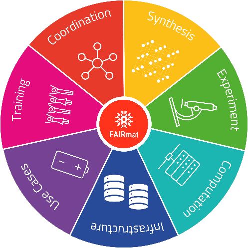
The FAIRmat consortium led by Humboldt-Universität zu Berlin describes its concept for accessible research data in the renowned journal Nature
How the FAIRmat consortium works (Copyright: FAIRmat)
The lifestyle of our society is largely determined by the achievements of condensed matter physics, chemistry and material sciences. Touch screens, batteries, electronics or implants: Many new products in the fields of energy, environment, health, mobility and information technology are largely based on improved or even novel materials. These fields generate enormous amounts of data every day, which is a new raw material - and is therefore a gold mine in itself. However, a prerequisite for this is that these data are comprehensively characterized and made available to science.
FAIR data for shared use
The FAIRmat consortium ("FAIR Data Infrastructure for Condensed-Matter Physics and the Chemical Physics of Solids"), led by IRIS Adlershof member Prof. Claudia Draxl, aims to refine this raw material, i.e. turning data into knowledge and value. A prerequisite is a data infrastructure that makes enables scientific data to be „FAIR", i.e. findable, accessible, interoperable and re-purposable. "With a "FAIR" infrastructure, data can be easily shared and explored using data analytics and artificial intelligence methods. This approach will significantly change the way how science is done today," says Claudia Draxl.
In the journal Nature, the scientists describe how such a data infrastructure can be successfully implemented in the field of materials science. The article appears today in the "Perspectives" format, in which the journal publishes forward-looking contributions that stimulate discussion and new scientific approaches.
The FAIRmat consortium is part of the initiative “Nationale Forschungsdaten Infrastruktur” (NFDI). The project is based on the extensive experience with the world's largest data infrastructure in computational materials science, the Novel Materials Discovery (NOMAD) Laboratory, which was co-founded by Claudia Draxl and has been online since 2014. The main challenge for FAIRmat is the integration of many different experimental characterization techniques and methods of material synthesis.
FAIR data enabling new horizons for materials research
M. Scheffler, M. Aeschlimann, M. Albrecht, T. Bereau, H.-J. Bungartz, C. Felser, M. Greiner, A. Groß, C.T. Koch, K. Kremer, W.E. Nagel, M. Scheidgen, C. Wöll, and C. Draxl
Nature 604 (2022) 635
DOI: 10.1038/s41586-022-04501-x
Contact:
Prof. Dr. Claudia Draxl
Institut für Physik / IRIS Adlershof
Humboldt-Universität zu Berlin
Tel.: 030 2093-66363
E-Mail: claudia.draxlphysik.hu-berlin.de
www.fairmat-nfdi.eu
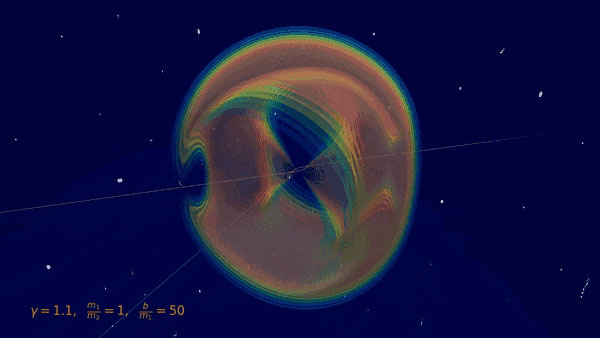
Fig 1: Visualization of the gravitational Bremsstrahlung from the scattering of two black holes (BSc thesis O. Babayemi)
When two massive objects (black holes, neutron stars, or stars) fly past each other, the gravitational interactions not only deflect their orbits, but also produce gravitational radiation, or gravitational bremsstrahlung, analogous to electromagnetism. The resulting gravitational waves of such a scattering event were calculated at leading order in Newton's gravitational constant in the 1970s using traditional methods of general relativity in an extensive series of four papers. Bremsstrahlung events are still out of reach for the current generation of gravitational-wave detectors because the signal is non-periodic and typically less intense. Nevertheless, they are interesting targets for future searches with future terrestrial and space-based observatories.
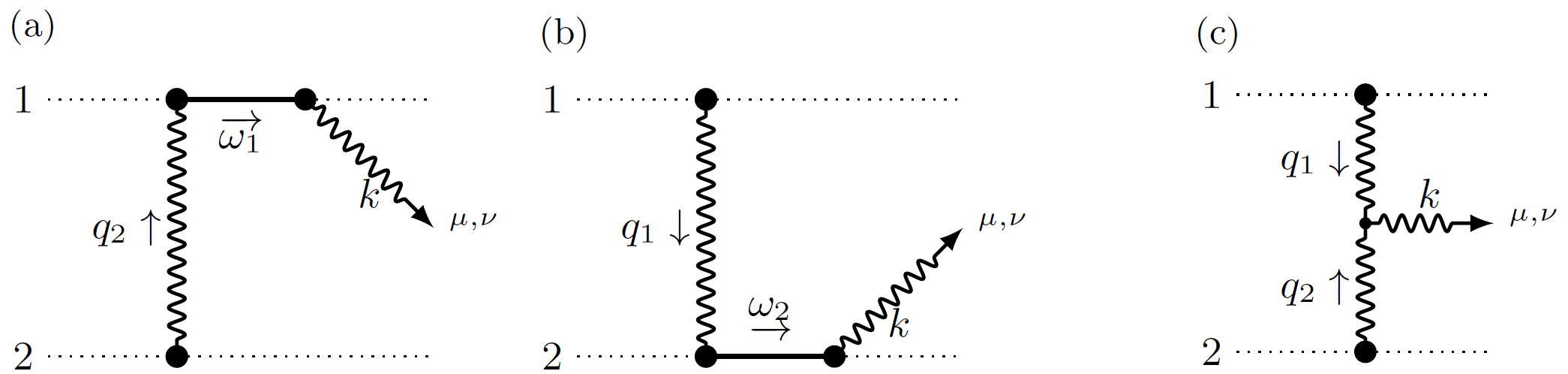
In the Quantum Field Theory lab around IRIS Adlerhof-member Prof. Plefka, a new approach to determining these waveforms (Fig. 1) and the deflections using methods of perturbative quantum field theory was recently developed, which proves to be significantly more efficient than the traditional approaches. It is based on a hybrid quantum field theory, in which the black holes (or stars) are idealized as point particles and interact with the gravitational field. The calculation is then based on a systematic diagrammatic expansion using Feynman graphs. I.e. the methods that were originally developed for the scattering of elementary particles can now also be used in astrophysical scenarios.
With this innovative method - the "Worldline Quantum Field Theory“ approach - our understanding of this fundamental physical process was recently significantly extended resulting in a series of three publications in the Physical Review Letters. In [1], the results from the 1970s were reproduced in a far more efficient way; this only required the calculation of three Feynman graphs (Fig. 2). In [2] the waveform could be extended to the case of rotating black holes and neutron stars. In a recent publication [3], the scattering angles and deflections in momenta and rotations due to the scattering process at the next-next-leading order of the gravitational constant were determined for the first time. Elaborated techniques for calculating Feynman integrals were used here. Interestingly, the rotational degrees of freedom of the black holes are described in this new formulation with a supersymmetric world line theory [4], which was originally developed in extensions of the Standard Model of particle physics.
This research was performed in the context of the DFG Research Training Group 2575 "Rethinking Quantum Field Theory“, where innovations in quantum field theory are developed in cooperation with the Max-Planck Institute for Gravitational Physics and the Helmholtz-Centre DESY.
Publikations:
| [1] | Classical Gravitational Bremsstrahlung from a Worldline Quantum Field Theory G. U. Jakobsen, G. Mogull, J. Plefka, and J. Steinhoff Phys. Rev. Lett. 126 (2021) 201103 arxiv: 2101.12688 OPEN ACCESS |
[3] | Conservative and radiative dynamics of spinning bodies at third post-Minkowskian order using worldline quantum field theory G. U. Jakobsen and G. Mogull erscheint in PRL arxiv: 2201.07778 OPEN ACCESS |
|
| [2] | Gravitational Bremsstrahlung and Hidden Supersymmetry of Spinning Bodies G. U. Jakobsen, G. Mogull, J. Plefka, and J. Steinhoff Phys. Rev. Lett. 128 (2022) 011101 arxiv: 2106.10256 OPEN ACCESS |
[4] | SUSY in the sky with gravitons G. U. Jakobsen, G. Mogull, J. Plefka, and J. Steinhoff JHEP 2201 (2022) 027 arxiv: 2109.04465 OPEN ACCESS |
Further Informationen:
Videos on Youtube (from BSc thesis of O. Babayemi)
Prof. Dr. Jan Plefka
Spokesperson RTG2575 „Rethinking Quantum Field Theory“
Dept. of Physics & IRIS Adlershof, Group Quantumfield- and Stringtheory
Email: jan.plefkahu-berlin.de
Tel: +49 (0)30 2093 66409
Sekr.: +49 (0)30 2093 66413
http://qft.physik.hu-berlin.de
https://www2.hu-berlin.de/rtg2575/
MORE SCIENTIFIC HIGHLIGTHS